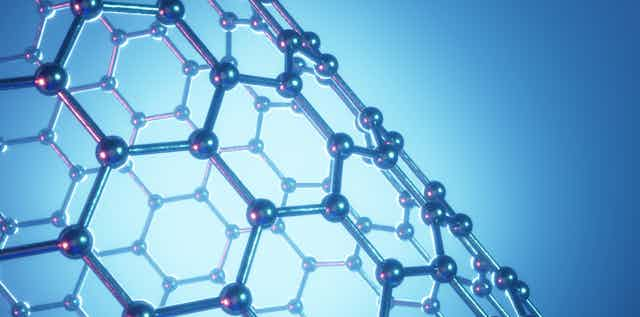
Graphene is a material made of carbon atoms one layer thick, arranged in a honeycomb structure. It has been used to make materials stronger, create ultra-high frequency components for communications, boost battery performance and even used to make COVID-19 tests. It’s the archetypal two-dimensional (2D) material – but there’s much more to 2D materials than graphene.
Since graphene was first isolated in 2004, research has expanded to the creation of other, non-carbon 2D materials. Now there are many tens of these, and they’re hailed to make an impact where graphene is less suited, such as in novel transistors and next-generation optoelectronic devices, which generate, detect and control light.
Our recent study focused on a new form of the 2D material tungsten disulfide (WS2), which is both 2D and 3D. WS2 is a semiconductor – the same as silicon, which is found in almost all electronic devices. However, unlike silicon, WS2 can exist in a stable 2D form. We arranged the WS2 material in a new way to create a 3D arrangement of 2D sheets that we call a nanomesh.
The WS2 nanomesh doubles the frequency and halves the wavelength of laser light – changing its colour as it does so – with great efficiency. This means it could be useful in components for quantum communications using light, where attempts to “eavesdrop” on messages can always be detected. Light is important in quantum communications because particles of light, called photons, can be used to carry information. When two photons experience something called quantum entanglement, anything that happens to one of them is immediately observable in the other, no matter how far apart they are.
Quantum communication has the potential to deliver truly secure communication across the world. Using the bizarre property of entanglement, it’s possible to engineer a system so that when a signal is intercepted, the sender immediately knows.
Many of the attempts so far to create quantum communications have been using laser light. But in order to do this we need an efficient way of controlling the light. This could potentially be done with 2D materials.

Two dimensional confinement
In 2D materials, electrons can move in two dimensions but their motion in the third dimension is restricted. This confinement gives 2D materials interesting properties that mean they show great promise as ultra-thin devices for IT, communications, sensing, energy, imaging and quantum computing. For many of these applications, the 2D materials, which are just one atom thick, lie flat on a supporting surface.
Unfortunately, however, the strength of these materials – that they are extremely thin – is also their greatest weakness. This means when they are illuminated, visible light can interact with them only over a tiny thickness and the resulting effect is weak. To overcome this, researchers like me are starting to look for new ways to pack the 2D materials into complex 3D structures.
Nanomesh
My PhD student and I created a webbed 3D network of densely-packed, randomly distributed stacks, containing rotated and fused 2D sheets called a nanomesh. Its unique characteristics are the result of the specific synthesis process we developed. We started by growing one-dimensional nanotubes (rolled sheets) of WS2, like a scaffold. These are naturally filled with a material from which WS2 sheets could grow at the nanotube tips and on their sides, rotated on top of each other and deployed like a fan. These sheets then fused with each other to create larger 2D sheets intersecting in 3D to create the nanomesh.
Read more: China's quantum satellite enables first totally secure long-range messages
Inside a semiconductor there are energy bands, separated by an energy gap. Only light with energy larger than the energy gap can interact with the material in a useful way. If new energy levels are introduced inside this energy gap, the doubling of frequency of the light that passes through the material is much more efficient and can take place over a larger range of wavelengths. This is exactly what our nanomesh achieves, it changes the energy landscape – the energy bands, energy gaps and energy levels inside the gap – of the material.
Measurements by my colleagues in the photonics group demonstrated the nanomesh material indeed efficiently converts one laser colour into another over a broad palette of colours. Compared to flat-lying WS2 layers, the nanomesh is highly efficient and responds to a wide range of light wavelengths, while also being durable and able to be grown over large areas.
Our study is proof that assembling 2D materials into a 3D arrangement doesn’t just result in thicker 2D materials with which the light interacts more strongly – it produces materials with entirely new properties.
The nanomesh we made is technologically simple to produce at large scale, and offers interaction with light that can be tuned. The material could be evolved further, for example by including small metallic nanoparticles or by depositing a second material. Such hybrids would offer additional ways to change laser light passing through them.
Our next goal is to incorporate the nanomesh into devices that transmit and modify light and which can be integrated with traditional microelectronics. This is a route for developing practical quantum optical communications.

