
What could we do with layered structures with just the right layers? What would the properties of materials be if we could really arrange the atoms the way we want them?
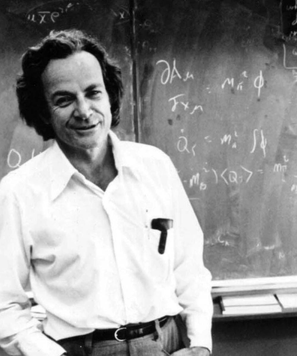
The curious American physicist Richard Feynman asked these questions in his landmark 1959 lecture, There’s Plenty of Room at the Bottom. It bustled with profound ideas about “manipulating and controlling things on the atomic scale”, using quantum mechanics.
Far-fetched at the time, now manipulating layers of atoms is a major research area. To realise Feynman’s vision, researchers at IBM and Bell Labs in the US had to devise a new approach to constructing materials layer by layer: molecular beam epitaxy or MBE.
This can be likened to spray painting with atoms. You start by vaporising ultra-pure source materials like gallium, aluminium or indium, and combine them with the likes of arsenic or phosphorus. The vaporised atoms fly through a vacuum chamber towards a base layer made of similar materials. The atoms stick to it and slowly build up a crystal one atomic layer at a time. The ultra-high vacuum ensures impurities are minimal.
Atomic architects
While the process is relatively slow – typically only a few atomic layers per minute – the precision is remarkable. It allows technicians to stack different semiconductor materials on top of each other to create crystals known as heterostructures, which can have extremely useful properties. By alternately stacking layers of aluminium arsenide and gallium arsenide, for example, you could produce a material that is extremely good at storing electricity.
Once this technique had been perfected in 1990s and 2000s, scientists were able to control the number of electrons and their energies in a particular crystal. And since light then interacts with these electrons, having more control over electron behaviour means you also gain more control of how they are stimulated by light.
Heterostructures have led to many new discoveries, particularly regarding the quantum behaviour of particles such as electrons within them. Nobel Prizes in Physics have been awarded five separate times (1973, 1985, 1998, 2000, and 2014), and the resulting materials have revolutionised civilisation.
Semiconductor heterostructures enable solar cells, LEDs, lasers and ultra-fast transistors. Even the internet would otherwise be impossible: the lasers which send the light pulses that encode the bits of information online are made from heterostructures, as are the photodetectors that measure these light pulses and decode the information.
There are restrictions, however. The atomic size, spacing and arrangement of these heterostructures cannot be too dissimilar between layers without defects arising. This limits the possible material combinations and the potential to freely engineer the electronic and optical properties.
Also, crystals naturally consist of atoms which form bonds in all three directions. This means there are always unsatisfied atoms with “dangling” bonds at the edges. Foreign impurities seek these bonds and create defects that can destroy other properties. This becomes especially important with smaller crystals, preventing them being integrated to their full extent into modern transistors, lasers and so forth.
Enter 2D crystals
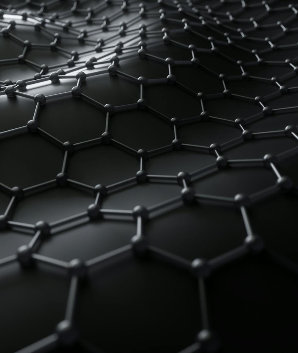
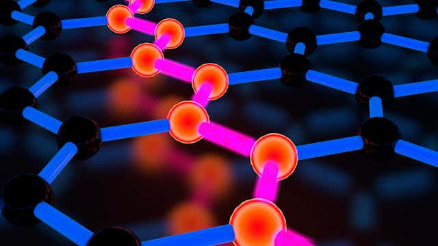
The ultimate in ultra-thin sheets of materials is a single layer of atoms. Fortunately, nature devised such “two-dimensional crystals”. The most famous is graphene, which is just carbon atoms arranged in a hexagonal pattern.
Graphene is stronger than steel and conducts electricity better than copper. It has many unique and sometimes exotic electronic, optical and mechanical properties – as recognised by the Nobel Prize in Physics for its discovery in 2010.
In a perfect graphene crystal, all the atoms are completely bonded to one another and there are no dangling bonds. It is famously possible to produce graphene by peeling apart layers of graphite using scotch tape: graphite is actually many layers of graphene all held together by Van der Waals forces, which are far weaker than the bonds in each constituent sheet of graphene.
Besides graphene, there are many other 2D crystals, each with unique properties. Several occur naturally as gems in the ground, such as molybdnimum disulphide, an important industrial lubricant. Others can be made by molecular beam epitaxy, such as the insulator boron nitride, and crystals in the same family of transition metal dichalcogenides as molybdnimum disulphide.
Like graphene is to graphite, scientists “peel off” (or exfoliate) single 2D sheets from larger quantities of these compounds. The inherent thinness of these sheets means they can behave quite differently from the heterostructures described earlier. Different atomically thin materials can be insulating, semiconducting, metallic, magnetic or even superconducting.
Scientists are also able to pick, place and combine these materials at will to form new heterostructures, known as Van der Waals heterostructures, with different properties to the 2D sheets. Crucially, these don’t have the same limitations as their cousins made by molecular beam epitaxy. They can comprise layers of very different atomic crystals, enabling unprecedented and unlimited possibilities for combining different materials.
For example, you can combine magnetic layers with semiconductors and insulators without attracting contaminants like moisture or oxides between layers – impossible with epitaxial heterostructures. This can be used to create devices that control magnetism using electricity, which is the basis for magnetic memory in hard drives.
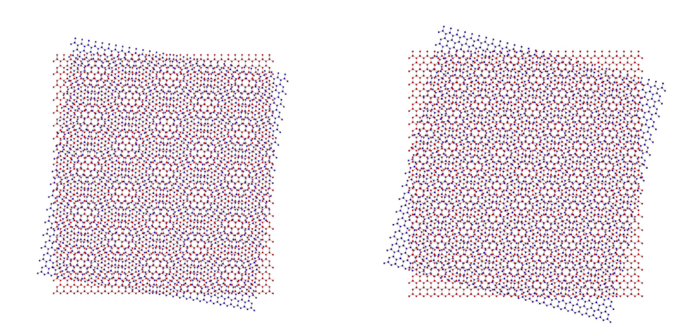
You can also stack together two identical atomic layers with one turned at an angle. This creates a lattice called a moiré pattern, which provides a new degree of freedom to engineer the electronic and optical properties. The images we are using to demonstrate this at the current Royal Society Summer Exhibition in London give a flavour of how this works:
While Van der Waals heterostructures are still in their infancy, impressive new physics and capabilities are already emerging. These include smaller, lighter, more flexible and more efficient versions of solar cells, LEDs, transistors and magnetic memory.
In future, we can expect surprises not previously dreamed of. An early example is the recent discovery that when you twist two layers of graphene at a “magic angle” relative to each other, the electrons become superconducting. This breakthrough, not clearly understood yet, could unlock 30-year-old mysteries of how electrons can navigate superconductors without losing any energy. It might allow us to use superconductors at room temperature, with potential benefits for everything from medical imaging and quantum computers to transmitting electricity long distances.
Predicting technological outcomes is not easy, however. As Herbert Kroemer, who shared the Nobel Prize in 2000 for developing semiconductor heterostructures used in high-speed and opto-electronics, often said:
The principal applications of any sufficiently new and innovative technology always have been and will continue to be applications created by that technology.