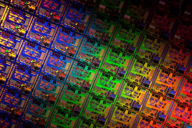
The semiconducting silicon chip launched the revolution of electronics and computerisation that has made life in the opening years of the 21st century scarcely recognisable from the start of the last. Silicon integrated circuits (IC) underpin practically everything we take for granted now in our interconnected, digital world: controlling the systems we use and allowing us to access and share information at will.
The rate of progress since the first silicon transistor in 1947 has been enormous, with the number of transistors on a single chip growing from a few thousand in the earliest integrated circuits to more than two billion today. Moore’s law – that transistor density will double every two years – still holds true 50 years after it was proposed.

Nevertheless, silicon electronics faces a challenge: the latest circuits measure just 7nm wide – between a red blood cell (7,500nm) and a single strand of DNA (2.5nm). The size of individual silicon atoms (around 0.2nm) would be a hard physical limit (with circuits one atom wide), but its behaviour becomes unstable and difficult to control before then.
Without the ability to shrink ICs further silicon cannot continue producing the gains it has so far. Meeting this challenge may require rethinking how we manufacture devices, or even whether we need an alternative to silicon itself.
Speed, heat, and light
To understand the challenge, we must look at why silicon became the material of choice for electronics. While it has many points in its favour – abundant, relatively easy to process, has good physical properties and possesses a stable native oxide (SiO2) which happens to be a good insulator – it also has several drawbacks.
For example, a great advantage of combining more and more transistors into a single chip is that it enables an IC to process information faster. But this speed boost depends critically on how easily electrons are able to move within the semiconductor material. This is known as electron mobility, and while electrons in silicon are quite mobile, they are much more so in other semiconductor materials such as gallium arsenide, indium arsenide, and indium antimonide.
The useful conductive properties of semiconductors don’t just concern the movement of electrons, however, but also the movement of what are called electron holes – the gaps left behind in the lattice of electrons circling around the nucleus after electrons have been pushed out.
Modern ICs use a technique called complementary metal-oxide semiconductor (CMOS) which uses a pair of transistors, one using electrons and the other electron holes. But electron hole mobility in silicon is very poor, and this is a barrier to higher performance – so much so that for several years manufacturers have had to boost it by including germanium with the silicon.
Silicon’s second problem is that performance degrades badly at high temperatures. Modern ICs with billions of transistors generate considerable heat, which is why a lot of effort goes into cooling them – think of the fans and heatsinks strapped to a typical desktop computer processor. Alternative semiconductors such as gallium nitride (GaN) and silicon carbide (SiC) cope much better at higher temperatures, which means they can be run faster and have begun to replace silicon in critical high-power applications such as amplifiers.
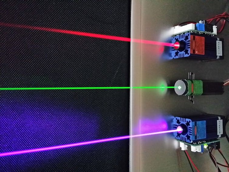
Lastly, silicon is very poor at transmitting light. While lasers, LEDs and other photonic devices are commonplace today, they use alternative semiconductor compounds to silicon. As a result two distinct industries have evolved, silicon for electronics and compound semiconductors for photonics. This situation has existed for years, but now there is a big push to combine electronics and photonics on a single chip. For the manufacturers, that’s quite a problem.

New materials for future
Of the many materials under investigation as partners for silicon to improve its electronic performance, perhaps three have promise in the short term.
The first concerns silicon’s poor electron hole mobility. A small amount of germanium is already added to improve this, but using large amounts or even a move to all-germanium transistors would be better still. Germanium was the first material used for semiconductor devices, so really this is a “back to the future” move. But re-aligning the established industry around germanium would be quite a problem for manufacturers.
The second concerns metal oxides. Silicon dioxide was used within transistors for many years, but with miniaturisation the layer of silicon dioxide has shrunk to be so thin that it has begun to lose its insulating properties, leading to unreliable transistors. Despite a move to using rare-earth hafnium dioxide (HfO2) as a replacement insulator, the search is on for alternatives with even better insulating properties.
Most interesting, perhaps, is the use of so-called III-V compound semiconductors, particularly those containing indium such as indium arsenide and indium antimonide. These semiconductors have electron mobility up to 50 times higher than silicon. When combined with germanium-rich transistors, this approach could provide a major speed increase.
Yet all is not as simple as it seems. Silicon, germanium, oxides and the III-V materials are crystalline structures that depend on the integrity of the crystal for their properties. We cannot simply throw them together with silicon and get the best of both. Dealing with this problem, crystal lattice mismatch, is the major ongoing technological challenge.
Different flavours of silicon
Despite its limitations, silicon electronics has proved adaptable, able to be fashioned into reliable, mass market devices available at minimal cost. So despite headlines about the “end of silicon” or the spectacular (and sometimes rather unrealistic) promise of alternative materials, silicon is still king and, backed by a huge and extremely well-developed global industry, will not be deposed in our lifetime.
Instead progress in electronics will come from improving silicon by integrating other materials. Companies like IBM and Intel and university labs worldwide have poured time and effort into this challenge, and the results are promising: a hybrid approach that blends III-V materials, silicon and germanium could reach the market within a few years. Compound semiconductors have already found important uses in lasers, LED lighting/displays and solar panels where silicon simply cannot compete. More advanced compounds will be needed as electronic devices become progressively smaller and lower powered and also for high-power electronics where their characteristics are a significant improvement upon silicon’s capabilities.
The future of electronics is bright, and it’s still going to be largely based on silicon – but now that silicon comes in many different flavours.

