Graphene, a single layer of carbon atoms, is being touted as the material that could change how electronics are made. But it’s difficult to make graphene in forms needed for electronics. Now, researchers from Stanford University have found a new method of making graphene by chemically converting DNA templates into flat sheets of carbon, potentially overcoming that limitation.
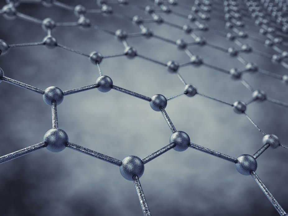
In graphene, carbon atoms are arranged in a hexagonal structure. This symmetrical structure is a good conductor of electricity. Shape it into ribbons narrower than 10 nanometres (billionths of a metre), though, and it can act as a semiconductor. If we can mass produce these thin ribbons, they could be used to build very small and efficient circuits and transistors, potentially making electronics cheaper, faster and smaller.
Many approaches to making narrow graphene ribbons have been reported in recent years. These vary from unzipping carbon nanotubes (a form of carbon that exists as tiny tubes), to burning away a layer of graphene in the presence of a mask bearing the right shape. Approaches in which the graphene is made via chemical reactions from simple starting materials have also been described. All of these approaches have been had limited success in producing long ribbons that are less than 10nm wide
The key innovation of the Stanford team was to use DNA as a template. DNA is readily available from natural sources and is easily manipulated into different shapes, from the narrow ribbons required here to elaborate 3D architectures dubbed “DNA origami”. It also binds readily to metal ions such as the copper catalyst used to convert methane to graphene.
Zhenan Bao and colleagues report these findings in the journal Nature Communications. Using a process called molecular combing, they extended bacterial DNA across a silicon wafer, forming the required shape. The team made both simple ribbons and overlapping crosses—in principle complex circuits could be designed in this way.
Once the DNA is in place, it is soaked in a solution of copper nitrate and heated to 800-1000 °C in the presence of methane and hydrogen gases. This starts a chemical reaction that leaves behind a graphene-like material in the shape of the DNA template. The non-carbon portions of DNA and the copper, which acts as a catalyst, evaporate in the furnace to give a pure product. Most importantly, the process forms ribbons less than 10nm wide.

There are some limitations. The graphene ribbons are not pure, crystalline graphene. Around 15% of the ribbon consists of non-crystalline carbon that lacks the electrical properties of graphene. This reduces the ability of the ribbons to act as semiconductors; in effect, the ribbons have resistors built into them at random points. (To emphasise this, the authors described the ribbons as graphitic, meaning graphene-like.)
Despite this, the researchers were able to build transistors out of the graphitic ribbons to demonstrate their potential applications. The presence of amorphous carbon means that high voltages must be applied to the ribbons before they will conduct. This reduces the useful lifetime of the graphitic material, and future work will certainly focus on modifying the chemistry so that it produces pure graphene.
The mechanism by which the ribbons form during heating is not yet understood. Still, this work is a creative solution to an important problem. If the process can be refined to give large amounts of pure graphene ribbons, the next generation of electronic devices may well be a step closer.

